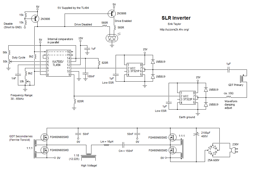
The Series Load Resonant (SLR)
topology is a switching topology which is particularly well suited to
handling
short circuits,
and ensures soft switching of the devices when powering a load. The
gist of it is to create a resonant circuit of the primary side of a
transformer, in which an external capacitor, optional external
inductor, and the leakage inductance of the transformer itself form
this resonant circuit. The switching devices are then run at half of
the resonant frequency, but at only 25% duty cycle. This may seem odd
at first, but consider that 25% duty cycle at f_res/2 is equal to one
half cycle of the resonant circuit. So in effect each switch pair will
only be on for a half cycle of the resonant circuit, and the deadtime
between turning on alternate pairs is equal to one half cycle. What
this does is allow the resonant circuit to ring up for half a cycle,
and then ring down without having extra energy added to the circuit. In
the meantime, the switching device can turn off once the current has
reversed/completed a half cycle, which is effectivly soft switching.
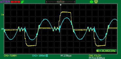
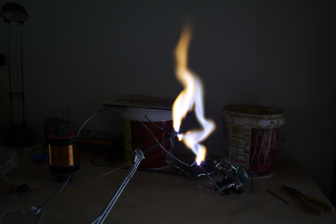
See the oscilliographs below. In the first the repetition frequency is
a little short, so there is some deadtime between each resonant cycle.
It can be seen that the circuit rings up while one switch pair is open,
and the switches close once the current has reversed and flows in the
diodes.
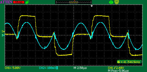
In the second the repetition frequency has been tuned so no deadtime
exists between each resonant cycle, which gives the greatest power
throughput. Soft-switching is ensured in both cases.
[Left] Transformer secondary is shorted. On-time a bit short, and frequency lower than f_res/2. [Right] On-time set correctly, and frequency at
f_res/2.
The requirement of f_res/2 and
25% duty cycle isn't the actual demand to the switch timing, but just a
coincidence. To maintain soft switching it is only required that the
switches turn off sometime after the current has reversed, but before
it has time to reverse twice, ie before the next full cycle can begin.
The deadtime between each pair of switches is turned on needs only be
longer than one full cycle. You could run the system at f_res/4 or even
some odd multiple, with the only result being that less power is
transferred through the circuit. This is the case in the first
oscilliograph above. The time the switches are left on for
however (one half cycle of the resonant circuit) must remain the same.
The peak value the current will swing to when
the secondary is shorted is given by the supply voltage divided by the
surge impedance Z_0 of the primary side resonant circuit. When lightly
loaded the current can swing up to twice this value again. (The peak
current seen in the waveforms above was taken during earlier tests with
different component values, so if you try the formula below using the
values given in the schematic they won't add up.)
Because of the timing
requirements needed for soft switching, using a
duty cycle and frequency controller like the TL494 is not ideal. The
best controller for this type of application would allow for the
on-time to be set rather than duty cycle, and the repetition
rate/frequency set independently. However, the TL494 works just fine
once
tuned correctly, and as it was what I had at hand it was used
here. Power regulation of the SLR converter is best done by using pulse
repetition modulation, where maximum power is processed at
f_res/2, and any frequency lower than this results in less power. This
isn't exactly possible with the TL494, but I made an enable input using
one of the error amplifiers none the less. This allows for the
connection of a crude hysteresis controller when charging capacitors to
some defined voltage. The enable input needs to be pulled low to
disable the controller, so a single NPN tranistor can be used for
electronic control.
Something I had originally
tried with this driver was to use UC3710T gate driver chips. I had
successfully used these before without issues, but in this driver I
experienced a sudden loss of gate drive which seemed to happen without
a specific cause. Shielding the driver seemed to help, but when trying
to charge a capacitor bank I would suddenly lose output from the
transformer, even though the driver was enabled.I eventually found that it was caused by latchup in the UC3710Ts, a problem some other people have experienced in the past.
Rather than attempt to fix an inherently flawed GDT driver design, I
simply changed over to UCC3732x gate drivers which have been used in
SSTCs for years. This fixed the problem immediately, even without
shielding the driver. I will not be usingUC3710Ts in any future designs, and recommend they are replaced in any old designs where present.
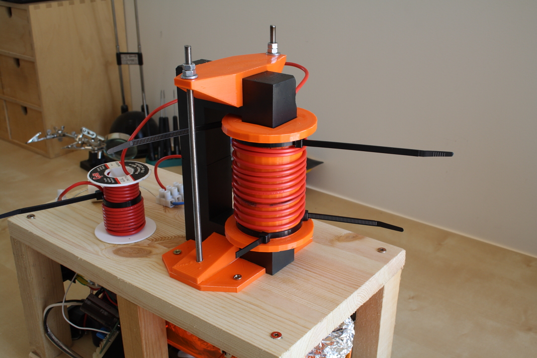
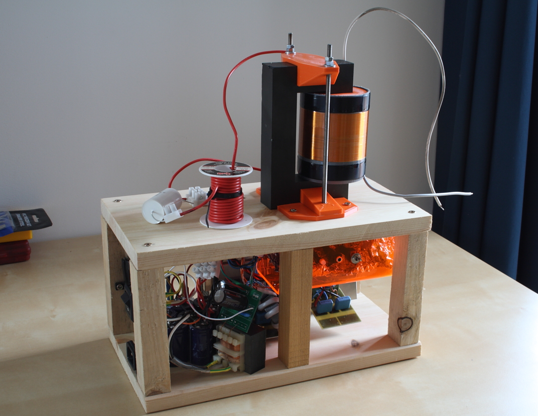
A major part of this project was just designing the transformer
itself.
From before I had the "Big mo-fo" transformer suspended in oil, and
simply run it using a hard switching inverter. The resulting voltage
spikes
from doing so made it almost impossible to insulate the transformer
properly,
and as a result it would often arc over to the core and burn off small
fragments of ferrite. This was even when under oil! It only felt good
to dismount the old
transformer, clean the oil from the core, and begin working on it from
scratch with a new design. Having acquired a 3D printer, it was
suddenly easy to create a
perfect core former to wind the primary on, and also hold the core
pieces together. I initially spent a lot of time calculating the
required number of turns and corresponding loss density in the core,
but once I started testing with the actual transformer I found it was
not the limiting factor in terms of losses. As things stand now, the
transformer may only rise 1 degree above room temperature in the time
it takes the secondary winding and external inductor to raise by 20
degress. I would also recommend you to wind the external inductor using
litz wire, if long run times are needed. The exact core I used was a
"EPCOS Core Set u/93/152/30" which
consists of two large U cores, material type N27. The number of primary
turns is 12, and the secondary consists of 1 layer of 0.25mm wire wound
on a 75mm diameter former. There are ca 225 turns on the secondary, and
the output voltage has been measured to 6kV peak. The secondary has
been placed above the primary winding in an attempt to minimize the
leakage inductance.
One may wonder why to minimize this "free" inductance, when it could
instead contribute to the total inductance on the primary side. The
reason I see for this is so that one has greater control over the power
delivered by the system. The peak current is given by the surge
impedance as shown above, and this again will depend on the inductance
and capacitance. If the leakage inductance is too large, the size of
the capacitor required to bring the surge impedance down to the desired
value may also bring the resonance frequency all the way into the
audible region. In addition to possible saturation problems at low
frequencies, ear splitting squeals from a transformer running 10+kVA is
no joke!
The 3D printed parts for the transformer were designed using OpenSCAD,
so they are completely parametric. They can be downloaded here,
and adapted to most transformer sizes.
Disclaimer:
I do not take responsibility for any injury, death, hurt ego, or other
forms of personal damage which may result from recreating these
experiments. Projects are merely presented as a source of inspiration,
and should only be conducted by responsible individuals, or under the
supervision of responsible individuals. It is your own life, so proceed
at your own risk! All projects are for noncommercial use only.


 This work is licensed under a
Creative Commons Attribution-Noncommercial-Share Alike 3.0 Unported License.
This work is licensed under a
Creative Commons Attribution-Noncommercial-Share Alike 3.0 Unported License.