My usual method of transferring a circuit from breadboard
to stripboard is tedious work, and if I wanted to use "just enough"
board space, I'd have to redo the layout several times. Since even
mediocre electronics hobbyists do their own PCBs, so I figured it's
about
time I started too. Not only would this allow me to design circuit
layouts on a PC where mistakes are free, but I could also use layouts
designed by other people. And
what tops off an electronics project more than soldering a PCB
you designed and created yourself? So I researched different PCB
production techniques, checked what my supplier had, and researched
some more. Toner transfer seemed to be the most commonly used method
among hobbyists, but I didn't have easy access to a laser printer, and
definitely not one I can stuff magazine pages into without getting in
trouble. The results seems to vary greatly depending on all sorts of
factors, and in the end you might not even get excellent trace
resolution. With toner transfer ruled out, the other options I had were
to draw my own traces with a marker (no thank you)
or use the photoresist method. Alright, so what are the downsides?
Start-up costs.
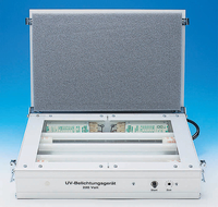
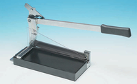
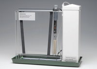
550 EUR for a UV box? 340 for a PCB guillotine? Another 500 for an
etching tank?
Fat chance. It's time to DIY.
The following materials are necessary for making a PCB:
Copper-clad board, with pre-sensitized photoresist
- Buy this from your electronics supplier, there's no
shortcuts here. There may be different copper thicknesses and board
materials available. I use FR4 board, 35 �m copper layer with
positive photoresist. It has worked well for all my projects so far.
Developer
- The photoresist will most likely be developed by
sodium hydroxide (NaOH). This is the main ingredient in most drain
cleaners,
so instead of paying for a 50g bag from your electronics supplier, go
to the grocery store and pick up a 500g bottle. In my case both cost
the same.
Etchant
- There are many choices available here. The most
common are ferric chloride, copper chloride and sodium persulphate. I
only have experience using sodium persulphate, but it hasn't left me
wishing for something else yet. It rather clean, easy to store, and
only fumes small amounts of oxygen while decomposing. The drawbacks are
slow etching speed and relatively high price.
In addition the following tools are also needed:
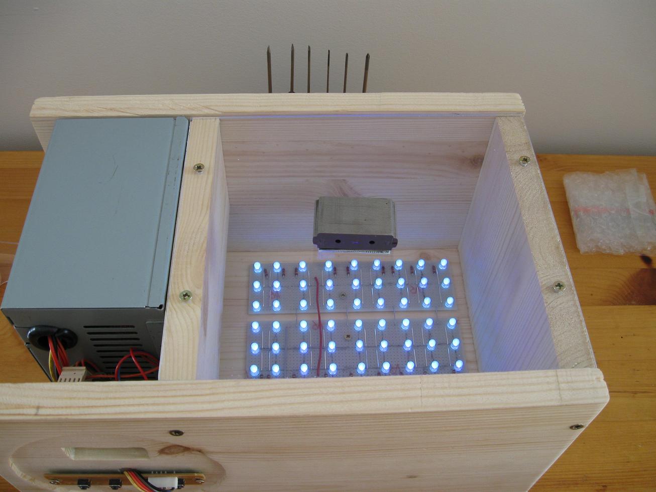
Means of UV exposure - Check out my UV LED exposure
box
to see what I did to create a means of exposing boards to UV. Otherwise
if you live close to the equator or under an ozone hole, I've heard of
people using sunlight. Not nearly as fast or reliable though.
Means of cutting copper-clad board
- The ideal solution here is to buy a PCB guillotine.
I haven't been able to convince myself it's worth the cost however, so
I use a common Stanley knife. What you do is score the board on both
sides first. I make sure to cut deeply, but this might not be
necessary. Once you've scored the board, simply put it in a vise, and
snap it!
Drillbits
- I also needed some
new
supplies to drill holes for through-hole components. FR4 board is made
of fiberglass, so it will dull common steel drill bits. Tungsten
carbide must be used if you want to get a decent lifetime out of your
drillbits. The stripboard I "grew up on" used 1mm holes, which fit for
almost any
component in my experience. So I purchased 1mm or #61 drill bits, and
some 1.5mm or #53 bits for wire connections and such. What you want to
look for when buying bits is resharpened carbide, these are cheap, and
often come with a standard 3mm shank so even the tiny 1mm bits can be
used by a standard drill chuck. Holes can be drilled by hand, but I
really recommend using a drill press. Keep in mind that glass dust will
be created when drilling fiberglass, so wear a dust mask. Running a
small shop-vac near your PCB while drilling is a good idea.
Once I had acquired the bare-bones minimum of tools and materials, it was time to test my setup. I created a
small PCB using (god-forbid) SMT. I wasn't happy with my previous
travel charger, and with my new PCB setup I suddenly had access to the
SMT chips, which almost all of the newer chips are sold as. For making the trace
mask/PCB-design I use ExpressPCB,
which is free. Make sure to adjust the component's hole size
according to the drill bits you have at hand, or you'll drill all the
copper away when making a hole. Also check that the component's lead
spacing is correct, the datasheet will always give exact measurements.
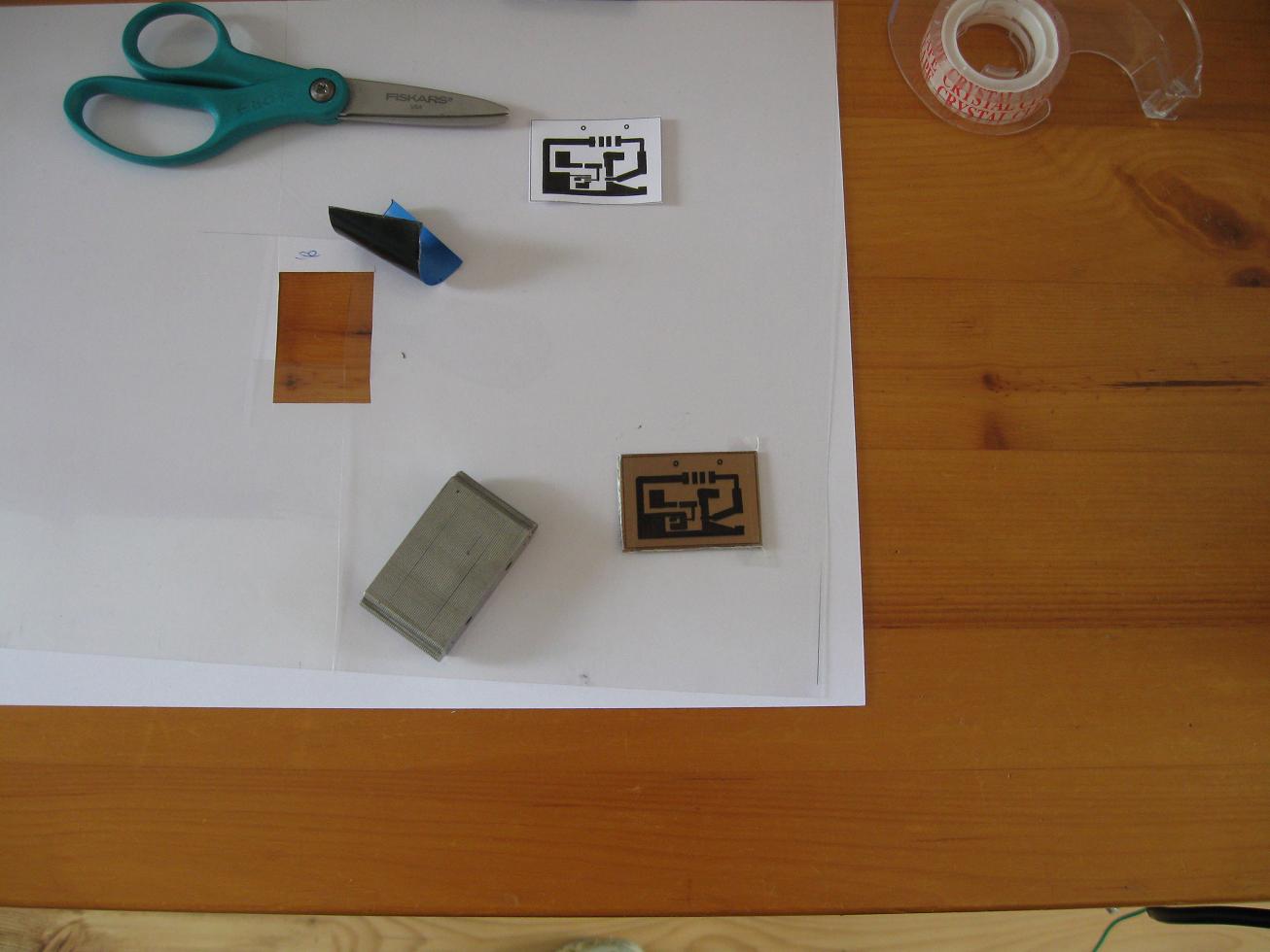
My
mom was so kind as to print the PCB mask on a sheet of overhead
transparency, which would
considerably lower the exposure time compared to paper. The trace mask
was taped to the PCB with clear scotch tape. For SMT
boards place the ink side up, and for through-hole the
ink side towards the board. Always double check that the mask is the
right way, otherwise your PCB will be mirrored. I set the timer for
2min and 30s on my first attempt. I
was unsure of the exact
time required, and didn't want to over-do it. At the same I had heard
of exposures taking 10 minutes or more with certain UV bulbs, so I
wasn't sure what to expect. From later exposures I've had best results
with exposure times near 6 minutes with transparencies, and 40 min and
up with standard
printer paper. Though printer paper takes a long time, it turns out
very
nicely, and the ink is dark enough to stop almost all of the UV so you
don't need to worry about overexposure. Some people soak the paper in
oil first to make it clearer, thus reducing exposure times. I weighted
the PCB down with some scrap iron to keep
the mask pressed tight to the PCB.
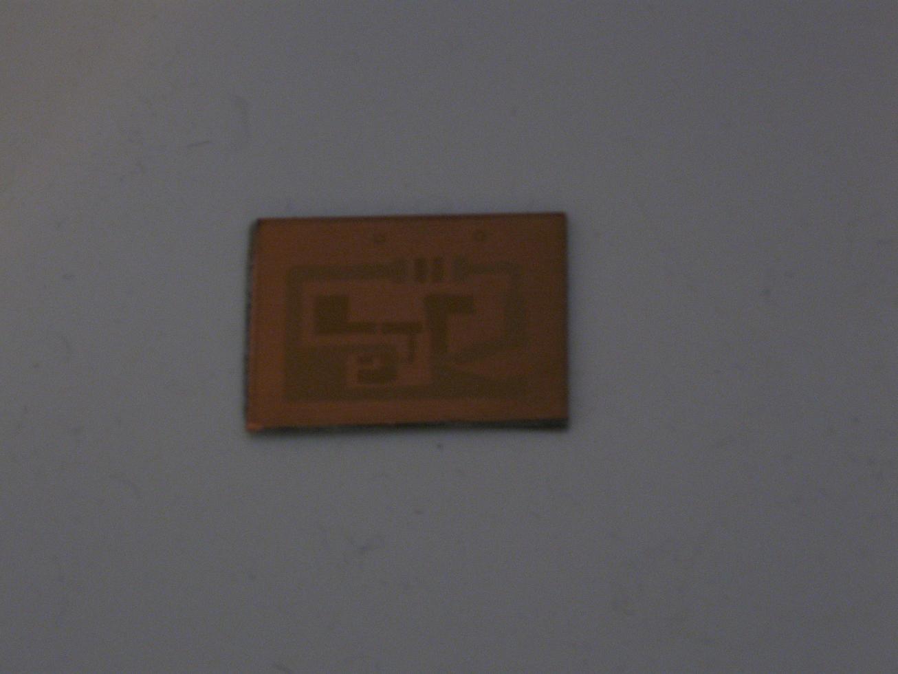
Picture is of the PCB after being developed in sodium
hydroxide.
After exposing the PCB, the unexposed traces will be slightly greenish
compared to
the exposed photoresist when viewed under bright light at an angle.
This is hard to see and requires optimal
lighting, so don't despair if you don't see anything. The traces should
become clearly visible after development however,
and the UV exposed photoresist should be removed entirely, revealing
fully exposed copper. To develop the exposed PCB I placed it in a
shallow bath of warm water, and slowly
added drops of concentrated NaOH solution. You'll need to add quite a
lot of NaOH before anything happens, but once it does can can
overdevelop the board it you're not careful. The
exposed photoresist will begin to dissolve once enough NaOH is added,
thus giving a brownish color to the
water. Depending on the quality of the photoresist your
board was coated with, the developer may not dissolve the unexposed
resist, or strip it off as soon as it's done with the exposed resist.
So watch this stage carefully.
When mixing dry NaOH crystals remember dissolving NaOH is an exothermic
reaction, so heat will be generated and can crack glass if too much is
mixed in at once. When mixing a batch of NaOH solution, I use precooled
water, and add a few crystals at a time. The first time I was
mixing up my solution I had a single drop of water fall into the NaOH
bag whilst there were some crystals left in it. I only noticed because
I felt
some extreme heat by my finger (which was holding th bag). A tiny drop
of water had dissolved a few crystals and created a supersaturated NaOH
solution, which had become almost hot enough to melt the thick plastic
bag. So mix the crystals into water,
and always use gloves and eye protection!
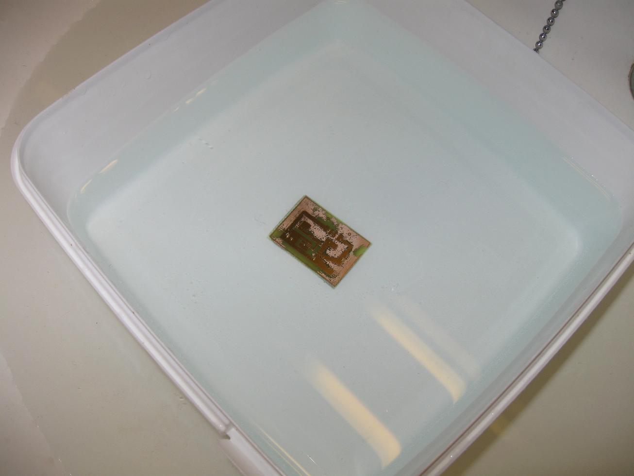
The next step is to place the board in the etchant. Sodium persulfate
etchant works best at 50C, so you need to keep the solution warm by
some means. I simply placed the etchant tub in a hot water bath, in the
bathroom sink. Exposed copper should go rosy/light pink within 2 minutes,
indicating the etchant is tarnishing it. If there is no change in
color, remove the PCB, wash it, and develop it some more. Reaction
speed is very dependent on temperature, and also dependent on how fresh
the etchant solution is. At room temperature expect at least 40 minutes
to
etch a board, while when closer to 50C it only takes 10-15 minutes.
Stir
occasionally, keeping bubbles off- and fresh solution on the
PCB. As the sodium persulfate is exhausted the solution will gradually
become deep blue with copper sulfate (CuSO4).
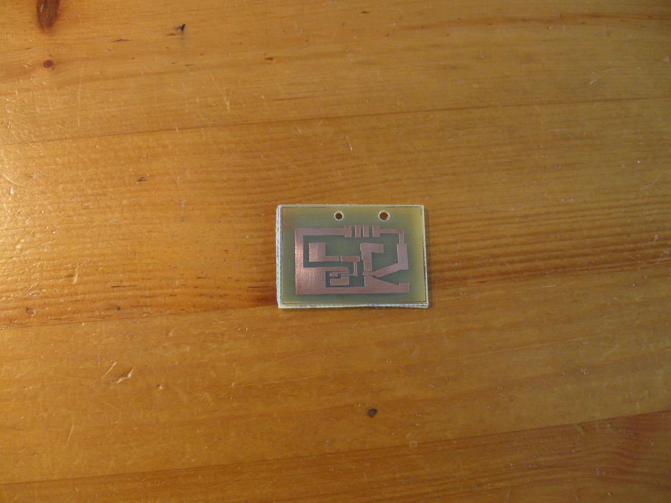
After etching, holes should be drilled since the photoresist will
protect the copper. Leave the resist on until you're ready to solder.
To remove the resist, you can either scrub it off with steel wool, or
if you can acquire NaOH cheaply, simply expose the PCB to UV (no mask this time) and
redevelop.
Here's the completed travel charger PCB. Notice even the tiny traces
outlining the PCB
turned out, and this was the first run without optimization! I can
definitely recommend this method to anyone who wishes to make their own
PCBs. It's clean, cheap, and fairly quick. And above all the PCBs turn
out great!
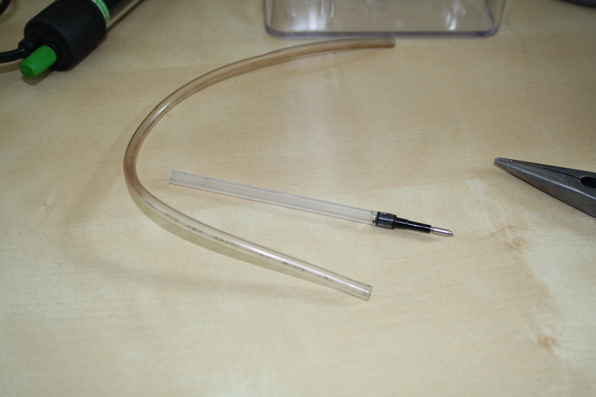
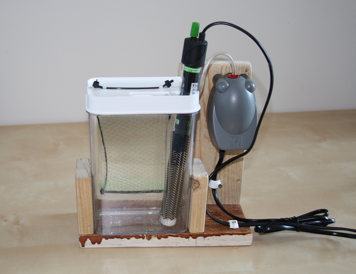
The
worst part of my PCB making process has been the etching. It works so
slowly, and the solution has to be heated using a hot water bath which
takes all eternity. Not only that, but I had to sit and stir the
solution by hand while the copper was being etched. To remedy this I
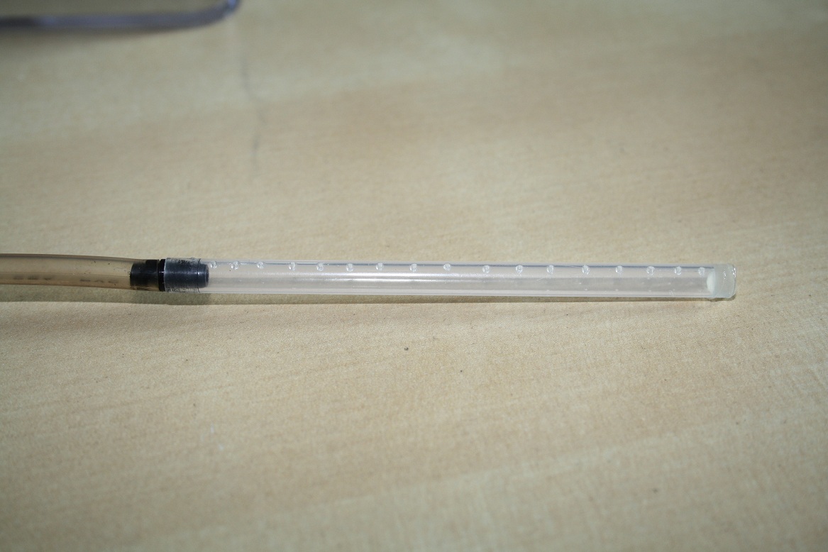
whipped up a little bubble tank, using some cheap aquarium components,
a 2$ container from the dollar store, a few zip ties and some odds and
ends. It's not handsome, but it is handy.
And
the results? The solution can now be heated to working temperature all
by itself while I expose the PCB. Not only that, but thanks to the
bubbles mixing the solution etch times have been halved! If you plan on
making more than two PCBs I demand you build something similar to save
yourself all the hassle of doing it by hand.
Disclaimer:
I do not take responsibility for any injury, death, hurt ego, or other
forms of personal damage which may result from recreating these
experiments. Projects are merely presented as a source of inspiration,
and should only be conducted by responsible individuals, or under the
supervision of responsible individuals. It is your own life, so proceed
at your own risk! All projects are for noncommercial use only.

 This work is licensed under a
Creative Commons Attribution-Noncommercial-Share Alike 3.0 Unported License.
This work is licensed under a
Creative Commons Attribution-Noncommercial-Share Alike 3.0 Unported License.