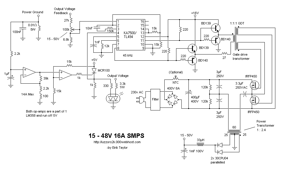
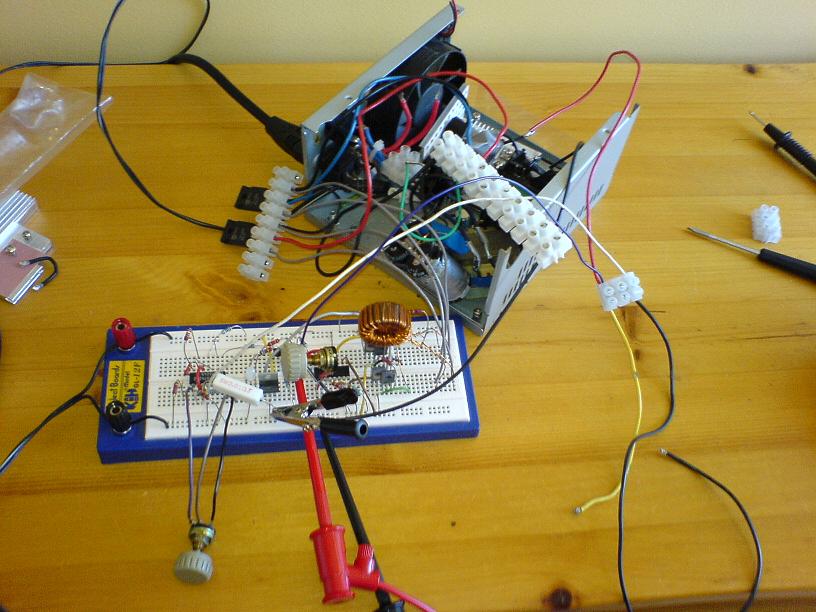
The
circuit operation is pretty straight-forward, and very modifiable.
The output voltage is compared with a stable reference voltage, and
based on the error the TL494 adjusts the duty cycle to compensate. The
output from the TL494 drives a BJT full-bridge, which drives the gate
drive transformer (GDT). The GDT controls the IRFP450 power mosfets.
The IRFP450s are in a half-bridge configuration and run the main power
transformer at the duty cycle decided by the TL494 chip. The output
from the main power transformer is rectified and filtered, and finally
the output voltage is measured again by the TL494. This is called
closed-loop operation. Each section of the circuit is dicussed further
down. I've made an
open-office spreadsheet
to aid modification or design, and all of the math I required is in it I believe. Just ask if something is missing.
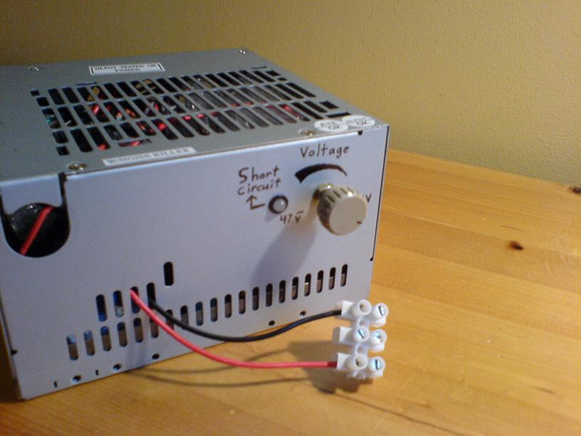
PWM Generation and Overcurrent detection Section
In my experience the logic section with GDT and fan(s) consumes about
15W +/- 5W. Keep this in mind when looking for a small 16V power
source. Iron-cored wall warts work well for this purpose. Pin 14 on the
TL494 generates a regulated 5V output, which is used for providing a
stable reference voltage. I do not use it for the 5V source in the
comparator section, as I don't want to load it down. One of the error
amps on the TL494 is used to determine the duty cycle. The reference is
divided by 2 with two 15k resistors and fed to pin 2 giving a 2.5V
reference. The output voltage from the supply is sent through a divider
as well, and depending on the potentiometer setting will provide an
output voltage of 2.5V at different voltages (15-48V). With low
resistance the ratio is low and it only takes 15V before the divider
output is 2.5V, high potentiometer resistance results in a large ratio
and high voltage required before 2.5v is reached. From pin 3 to pin 2
is a gain compensation network, consisting of a capacitor and resistor.
The purpose of this is to stabilize the control loop, and it's design
is far too complex for amatures to understand. (I haven't even tried.)
All you need to know is that the capacitor's impedance will vary with
frequency, in effect giving a frequency dependent resistor. This
coupled with the 180k resistor gives the error amp frequency dependent
gain, allowing for stabilization depending on the load, duty cycle and
frequency. Like I said, you don't want to know.
The overcurrent detection works by sensing current with a shunt
resistor, which is a resistor from your load to real/circuit ground.
Thanks to Ohm's Law (U=R*I <--this is too easy) we know that
with a set current and resistance, the voltage developed across the
resistor is known. Just a note to the circuit, power ground is the
negative lead out from your supply, you can't use ground as the
negative supply lead if you want overcurrent protection. The voltage
developed across the resistor is fed through an RC filter which
slows it down and keeps the mean value, and later amplified by the
first op-amp. Amplification reduces the voltage needed across the
resistor, which greatly reduces it's losses. The gain of the first
op-amp is set with the 3 resistors around it (39k, 2.2k and 100R) and
depending on the gain different overcurrent levels can be chosen. The
second op-amp
acts as a comparator and trips the small SCR when the current limit is
exceeded, lighting the warning LED at the same time. Just like with the
TL494 error amp you set a reference voltage on the inverting input with
a voltage divider, and feed the signal into the non-inverting input.
The funky dual LED will light one of it's didoes when an overcurrent
condition occurs, while the other diode will lose power since it's
powered from the main supply.
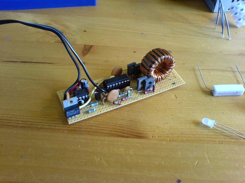
Gate Drive Section
The output section in the TL494 consists of two transistors, which
cannot drive a transformer directly. So by using some pull-up resistors
it can drive a full-bridge of small BJTs, which can then drive a
GDT. The design of the full bridge and TL494 outputs is such that
during deadtime both primary leads of the GDT will be held low. This is
equivalent to shorting the core, which resets it and allows for
flawless duty cycle generation through a transformer. Toroidal ferrite
cores with high Al value and decent cross-sectional area (50-100mm^2)
are excellent for GDT creation. At low frequency operation such as this
quite a few turns are required. Although the voltage stand-off isn't
optimal, and some cores are sharp enough to scratch off enamel I've
used magnet wire for winding my GDT. In high frequency applications I
use multi-strand coax cable, which gives the best performance. See how
you feel about the core and safety when you choose materials. James
Pawson has a great site on
GDT making (among other things).
POWER Section
Rectified mains is filtered (this is optional) mainly to keep noise
from the supply from traveling back up mains and disturbing other
appliances. I built an unregulated and sloppy SMPS for an amplifier
before this project, without a filter of course, and whenever I turned
it on my brother's amplifier in another room would start humming. So
yes, it is somewhat important. Mains is rectified with a beefy bridge
and filtered with a large storage capacitor. Between the bridge and
capacitor is a NTC. NTCs have a negative thermal coefficient, hence the
name. What they do is have low resistance at high temperature, and high
resistance at low temp. In this circuit one is used to limit the inrush
current to the man filter capacitor. Since a large capacitor will
provide a substantial load when empty, it can draw enough current when
starting up the PSU to blow fuses or a breaker. The NTC prevents this
by limiting the initial current, and slowly letting more through as it
heats up. The problem is that when drawing 500W or more large NTCs
are needed which aren't easy to find or very practical, so the NTC can
be omitted. If the filter capacitor causes your breaker to trip use a
light-bulb/switch like in my MKII multipurpose inverter. The two 120k
resistors simply bleed away charge on the filter capacitor when the
supply is turned off.
From the GDT outputs come alternating square-wave pulses 180 degrees
out of phase, which control the IRFP450s. Together with the two
3µF capacitors they form a half-bridge, which sends alternating
current through the main power transformer. The two 3µF
capacitors will carry all of the load current, and should be
polypropylene foil type capacitors. Some designs use electrolytics for
the half-bridge and filter capacitors in one, but I've found that the
electrolytic heat up and eventually fail when used this way. The amount
of average
current sent through the transformer is controlled by the duty cycle,
which is controlled by the TL494. The secondary is center-tapped so
dual diode rectification can be use. For filtration of the rectified
output a 33µH inductor and 1000µF capacitor are used. The
double 400V 16A rectifiers seem to be
overkill, but I found them necessary. They were reasonably cheap
anyway.
Experiments with 60V Schottky diodes resulted in plenty of
failures for some unknown reason, so I would go no lower than 100V, and
rate the diodes
generously for the current. This is your workhorse remember!
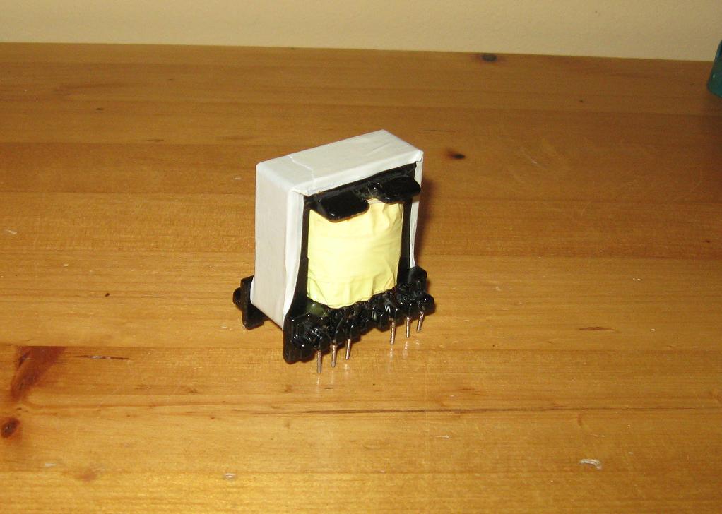
The power transformer itself was put together from an old ATX core,
which is ideal since they are used in this exact same fashion and
frequency. They might not be large enough for continuous operation at
more than 300W, but enough to last shorter runs at twice that. A good
question is how to design a transformer for 750W operation. What
limits power in transformers is how much power they can dissipate.
A core can lose power through losses tied to drive frequency and/or
magnetic flux being too high, but that's about it unless I'm mistaken.
The other losses are copper losses from the windings, and ideally you
want to fill the entire window area with copper to reduce the
resistance as much as possible. So if you can the required number of
turns in at the required thickness in the winding area, the core is
large enough. The resistance of the wires, even if only 0.5 ohms can
drop a decent amount of voltage. Now the DC resistance might seem low,
but remember that the skin effect kicks in too, increasing the
effective AC resistance. At 45kHz, for 16A capable wire I would use
four strands of 22AWG twisted together as litz wire. The primary only
has to handle about 4-5A at full load, so bifilar 22AWG should be
enough.
For further reference see these projects. They were of great use during the design process of my bench supply.

 This work is licensed under a
Creative Commons Attribution-Noncommercial-Share Alike 3.0 Unported License.
This work is licensed under a
Creative Commons Attribution-Noncommercial-Share Alike 3.0 Unported License.